1. Power Supply
Check if the supply voltage is correct and stable.
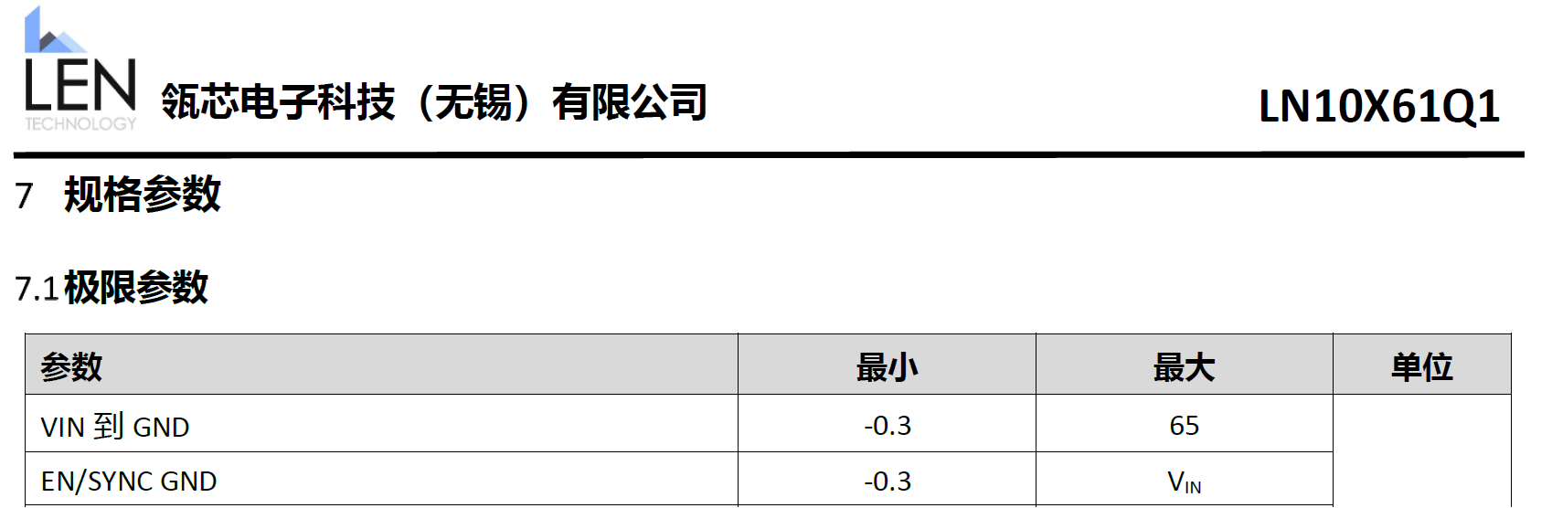
2. Inductor
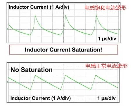
Verify the inductance value, saturation current, and temperature rise current margin. Insufficient ratings may lead to inductor saturation.
-
It is recommended to use a 2.2 µH–22 µH inductor with a saturation current higher than the LN10X61Q1 peak current limit (ILIM-PK).
-
Inductance value determines ripple current:
Higher inductance → smaller ripple current → lower output voltage ripple (with the same output capacitor)
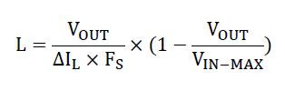
3.Lower inductance → larger ripple current
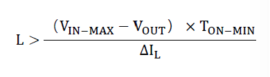
We recommend keeping ripple current (ΔIL) within 20%–40% of the rated output current, using the following calculation formula:
3.Enable
Check if the EN pin is active and the chip is operating. Refer to the datasheet—most chips use high-level enable, while some support floating EN for default enable.
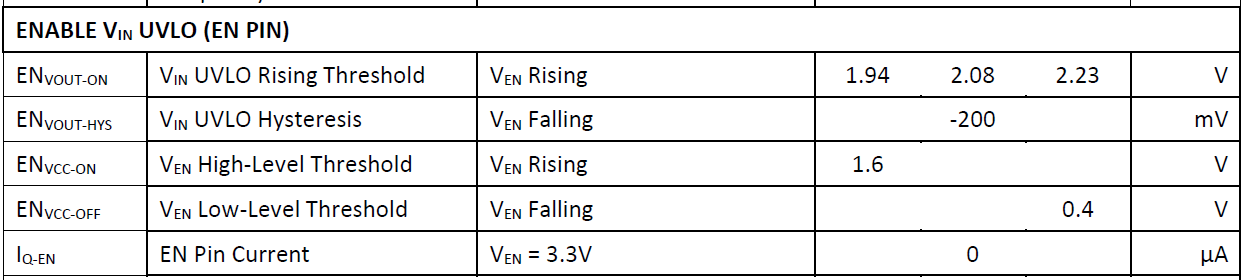
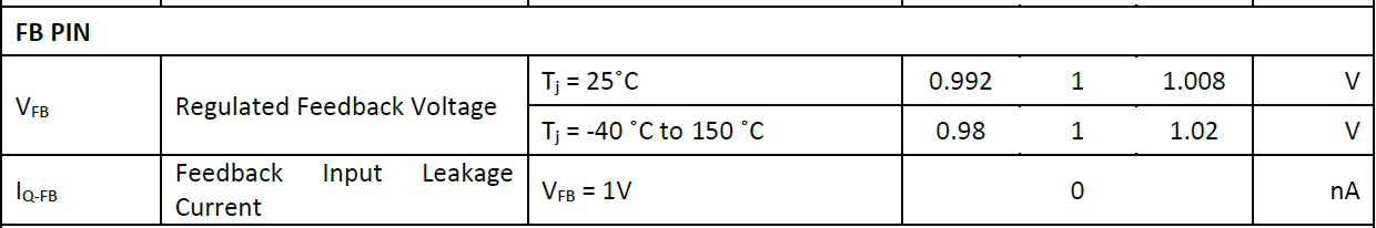
4.Feedback
Check if the FB pin voltage is correct, if there are any cold solder joints, and whether the feedback resistors are soldered with the correct values.
Datasheets usually provide recommended resistor values—too large may cause inaccurate output voltage or loop instability.
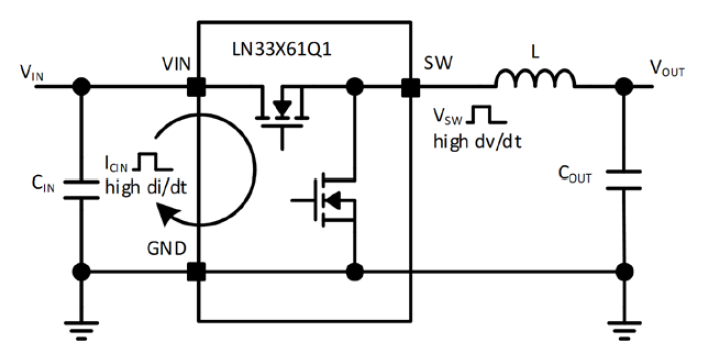
5.Bootstrap Capacitor
In synchronous buck converters (only with a high-side NMOS), poor soldering, too small capacitance (typically 0.1 µF–1 µF ceramic, ≥6.3 V), or excessive duty cycle leading to insufficient charging can all prevent the NMOS from turning on and cause output issues.
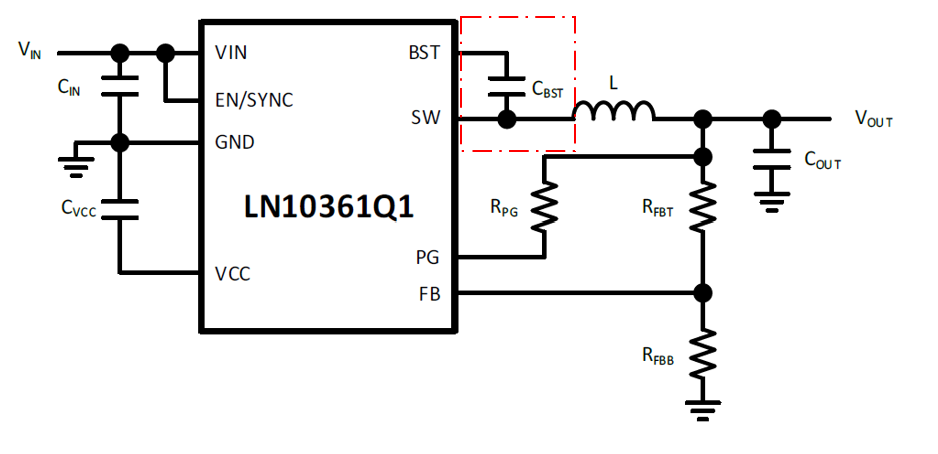
6.Layout Recommendations
For best performance and low EMI, place a high-frequency bypass capacitor as close as possible to VIN and GND pins to minimize loop inductance.
Keep SW traces short and away from sensitive signals.
Use wide, short traces for high-current paths (VIN, VOUT, GND).
Prefer a multi-layer PCB with solid GND planes and good thermal vias under the chip for heat dissipation.
Place high-frequency ceramic bypass capacitors (CIN) as close as possible to the LN10361Q1 VIN and GND pins to minimize high-frequency input loop area. For multiple input capacitors, position small-package ones (e.g., 0603) nearest to the pins for optimal high-frequency noise suppression.
Use wide, short traces for high-current loops (VIN, VOUT, GND).
Place the VCC bypass capacitor close to its pin and connect it back to the chip’s GND with the shortest path.
Use a 4-layer PCB with 2 oz copper on top/bottom and 1 oz on inner layers. Connect the LN10361Q1 thermal pad to all layers with via arrays. Make the first inner layer a solid ground plane for both heat dissipation and shielding. Maximize ground copper on all layers.
Keep SW network traces short and wide to carry current while minimizing high-frequency noise.
——————————————————————————————
Service:


 Wechat
 销售在线
销售在线 联系电话
联系电话